Fil:Gerber-layers-example.png
Storlek på förhandsvisningen: 139 × 599 pixlar. Annan upplösning: 232 × 1 000 pixlar.
Originalfil (232 × 1 000 pixlar, filstorlek: 157 kbyte, MIME-typ: image/png)
| Denna fil tillhandahålls av Wikimedia Commons. Informationen nedan är kopierad från dess filbeskrivningssida. |
| Beskrivning | Board design and Gerber file format image |
| Datum | |
| Källa | en.wikipedia.org/..Gerber-layers-example.png |
| Skapare | en:User:Halley |
| Tillstånd (Återanvändning av denna fil) |
Public domain |
| Andra versioner |
 |
Sammanfattning
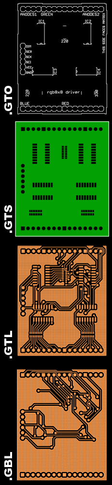
Board design and Gerber file format image created by Ed Halley, custom for Wikipedia article Gerber File.
Example Gerber layers, showing:
- .GTO file describes the top overlay (silkscreening to document the parts)
- .GTS file describes the top solder resist (a protective film to avoid stray solder)
- .GTL file describes the top layer copper traces (the rest is etched away)
- .GBL file describes the bottom layer copper traces of a printed circuit board.
Not shown: any silkscreening or solder resist on the bottom of the board, and a definition of all drill sizes and locations. Some designs may also have more copper layers sandwiched between boards.
Licensiering
| Jag, upphovsrättsinnehavaren till detta verk, släpper detta verk i public domain. Detta gäller globalt. I vissa länder kan detta inte vara juridiskt möjligt; i så fall: Jag ger härmed envar rätten att använda detta verk för alla ändamål, utan några villkor, förutom villkor som lagen ställer. |
Filhistorik
Klicka på ett datum/klockslag för att se filen som den såg ut då.
| Datum/Tid | Miniatyrbild | Dimensioner | Användare | Kommentar | |
|---|---|---|---|---|---|
| nuvarande | 12 januari 2010 kl. 18.53 | 232 × 1 000 (157 kbyte) | Bitsrc | {{Information |Description=Board design and Gerber file format image |Source=[http://en.wikipedia.org/wiki/File:Gerber-layers-example.png en.wikipedia.org/..Gerber-layers-example.png] |Date=19:47, 8 February 2009 |Author=en:User:Halley |Permission=Pu |
Filanvändning
Följande sida använder den här filen:
Global filanvändning
Följande andra wikier använder denna fil:
- Användande på da.wikipedia.org
- Användande på ja.wikipedia.org